As semiconductor companies increasingly develop highly customized silicon solutions, the demand for advanced backend implementation and full-chip integration expertise continues to grow. VNCHIP Labs provides end-to-end Spec-to-GDSII design services that transform architecture concepts into production-ready silicon.
Our services include SoC architecture support, IP integrationIP integration
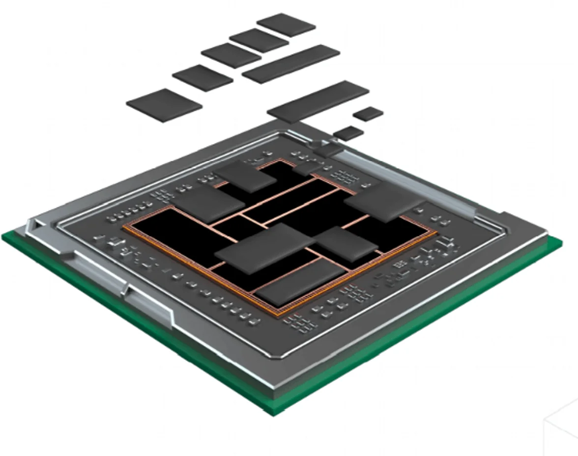
VNCHIP Labs provides comprehensive IP integration services for complex SoC and chiplet designs, enabling seamless integration of customer-developed IPs, VNCHIP Labs IPs, and third-party commercial or open-source IPs into a unified system architecture. Our engineering teams design and optimize interconnect fabrics, Network-on-Chip (NoC) architectures, bridges, and subsystem connectivity to meet performance, power, scalability, and integration requirements.
We support both industry-standard and custom protocols, including AXI, AHB, APB, CHI, PCIe, CXL, UCIe, Ethernet, and proprietary interfaces. Our services include protocol adaptation, clock and reset integration, address-map definition, coherency integration, bandwidth optimization, verification, timing closure support, and system-level validation to ensure reliable operation across heterogeneous IP environments., RTL developmentRTL Development/Refinement
VNCHIP Labs provides RTL development and refinement services for SoCs, ASICs, chiplets, and subsystem designs across AI, networking, data center, automotive, and edge applications. Our engineering teams can develop original RTL implementations based on customer-provided architecture and microarchitecture specifications, delivering scalable, synthesizable, and verification-ready designs optimized for performance, power, and area goals.
In addition to new RTL development, VNCHIP Labs offers RTL refinement services to enhance existing or incomplete RTL implementations. This includes improving functionality, performance optimization, protocol compliance, code restructuring, timing-aware modifications, low-power enhancements, debug support, and integration readiness. Our teams work closely with customers to accelerate development schedules while improving design quality, maintainability, and first-silicon success., verificationDesign verification
VNCHIP Labs provides comprehensive design verification services using advanced UVM-based verification methodologies to validate RTL implementations against architecture and microarchitecture specifications. Our teams develop scalable verification environments, testbenches, protocol monitors, scoreboards, assertions, and coverage-driven regression infrastructures that thoroughly stimulate and validate functional correctness across complex SoC and IP designs.
To accelerate verification closure, VNCHIP Labs leverages AI-assisted automation and intelligent verification agents to improve testcase generation, regression analysis, bug triage, and coverage optimization. By combining traditional verification expertise with AI-driven workflows, we help customers achieve verification milestones faster while improving functional, code, and assertion coverage metrics, reducing overall verification cycle time and increasing first-silicon confidence., prototypingPrototyping
VNCHIP Labs provides FPGA-based prototyping services to help customers validate IPs, subsystems, and critical portions of complex SoC designs before silicon availability. Our teams can implement customer IPs and system architectures on FPGA platforms to enable high-speed functional validation, software development, performance analysis, and early ecosystem integration.
We develop drivers, firmware, and validation software to exercise the design at realistic operating speeds and to interface with actual partner or third-party devices and platforms. In addition, VNCHIP Labs supports software bring-up, application development, and customer driver validation using the prototyping environment, allowing hardware and software teams to identify issues early, accelerate system integration, and reduce overall silicon development risk., power and performance analysisPower and performance analysis
VNCHIP Labs provides power and performance analysis services to help customers evaluate their designs against key application workloads and system use cases. Our teams analyze architecture behavior, data movement, memory bandwidth, latency, interconnect efficiency, and compute utilization to identify performance bottlenecks and estimate dynamic and static power consumption under realistic operating conditions.
Using simulation, profiling, emulation, and workload-driven analysis techniques, we help customers understand tradeoffs between performance, power, area, and thermal constraints early in the development cycle. Based on the analysis results, VNCHIP Labs can recommend architectural, RTL, clocking, memory, and interconnect optimizations to improve system throughput, reduce latency, and lower overall power consumption while maintaining design goals and implementation feasibility., physical implementation, STA/DFT signoffSTA/DFT signoff
VNCHIP Labs provides comprehensive STA and DFT signoff services to ensure designs meet timing, testability, reliability, and manufacturability requirements before tapeout. Our physical implementation teams perform detailed analysis and verification throughout the backend flow, including timing constraint validation, multi-mode multi-corner (MMMC) static timing analysis, clock-domain crossing checks, signal integrity analysis, IR drop and electromigration evaluation, power integrity verification, noise analysis, thermal assessment, and physical design rule compliance.
For DFT signoff, we support scan insertion, ATPG generation, scan compression, memory BIST integration, JTAG/debug infrastructure, test coverage analysis, and manufacturing test readiness validation. During implementation and signoff, VNCHIP Labs conducts extensive backend verification iterations to identify and resolve timing violations, congestion issues, routing challenges, DRC/LVS violations, testability gaps, and ECO-related issues. Our disciplined signoff methodology helps customers achieve reliable first-silicon success and production-ready GDSII handoff for fabrication., and final GDSII handoffGDSII handoff
VNCHIP Labs provides comprehensive GDSII handoff services to ensure designs are fully verified, properly configured, and ready for successful fabrication. Prior to tapeout, our teams perform final implementation reviews and signoff checks covering all physical design layers, process technology rules, timing constraints, power integrity, manufacturability requirements, and foundry-specific configurations.
We work closely with customers through structured tapeout readiness reviews to validate DRC/LVS closure, STA signoff, antenna checks, density verification, IR/EM analysis, metal fill insertion, packaging interface requirements, and final netlist-to-layout consistency. Our methodology ensures that all design databases, masks, configuration files, and deliverables are aligned with foundry requirements before final GDSII release. This disciplined review and handoff process helps reduce fabrication risk and improves confidence in first-silicon success.. With experience across advanced-node FinFET technologies and complex SoC designs, we help customers optimize performance, power, area, and development schedule for AI, networking, data center, automotive, and edge applications.
VNCHIP Labs supports both turnkey silicon development and targeted engineering engagement models, delivering disciplined execution from specification through tapeout.
VNCHIP Labs provides comprehensive RTL-to-GDSII implementation services for complex SoCs, ASICs, and chiplet-based designs. Starting from customer RTL, our teams support IP integration, RTL development refinementRTL Development/Refinement
VNCHIP Labs provides RTL development and refinement services for SoCs, ASICs, chiplets, and subsystem designs across AI, networking, data center, automotive, and edge applications. Our engineering teams can develop original RTL implementations based on customer-provided architecture and microarchitecture specifications, delivering scalable, synthesizable, and verification-ready designs optimized for performance, power, and area goals.
In addition to new RTL development, VNCHIP Labs offers RTL refinement services to enhance existing or incomplete RTL implementations. This includes improving functionality, performance optimization, protocol compliance, code restructuring, timing-aware modifications, low-power enhancements, debug support, and integration readiness. Our teams work closely with customers to accelerate development schedules while improving design quality, maintainability, and first-silicon success., verificationDesign verification
VNCHIP Labs provides comprehensive design verification services using advanced UVM-based verification methodologies to validate RTL implementations against architecture and microarchitecture specifications. Our teams develop scalable verification environments, testbenches, protocol monitors, scoreboards, assertions, and coverage-driven regression infrastructures that thoroughly stimulate and validate functional correctness across complex SoC and IP designs.
To accelerate verification closure, VNCHIP Labs leverages AI-assisted automation and intelligent verification agents to improve testcase generation, regression analysis, bug triage, and coverage optimization. By combining traditional verification expertise with AI-driven workflows, we help customers achieve verification milestones faster while improving functional, code, and assertion coverage metrics, reducing overall verification cycle time and increasing first-silicon confidence., prototypingPrototyping
VNCHIP Labs provides FPGA-based prototyping services to help customers validate IPs, subsystems, and critical portions of complex SoC designs before silicon availability. Our teams can implement customer IPs and system architectures on FPGA platforms to enable high-speed functional validation, software development, performance analysis, and early ecosystem integration.
We develop drivers, firmware, and validation software to exercise the design at realistic operating speeds and to interface with actual partner or third-party devices and platforms. In addition, VNCHIP Labs supports software bring-up, application development, and customer driver validation using the prototyping environment, allowing hardware and software teams to identify issues early, accelerate system integration, and reduce overall silicon development risk., power and performance analysisPower and performance analysis
VNCHIP Labs provides power and performance analysis services to help customers evaluate their designs against key application workloads and system use cases. Our teams analyze architecture behavior, data movement, memory bandwidth, latency, interconnect efficiency, and compute utilization to identify performance bottlenecks and estimate dynamic and static power consumption under realistic operating conditions.
Using simulation, profiling, emulation, and workload-driven analysis techniques, we help customers understand tradeoffs between performance, power, area, and thermal constraints early in the development cycle. Based on the analysis results, VNCHIP Labs can recommend architectural, RTL, clocking, memory, and interconnect optimizations to improve system throughput, reduce latency, and lower overall power consumption while maintaining design goals and implementation feasibility., and complete backend physical implementation through final tapeout.
Our implementation flow includes synthesis, scan insertion, floorplanning, placement and routing, clock-tree synthesis, timing closure, signal integrity analysis, and STA/DFT signoffSTA/DFT signoff
VNCHIP Labs provides comprehensive STA and DFT signoff services to ensure designs meet timing, testability, reliability, and manufacturability requirements before tapeout. Our physical implementation teams perform detailed analysis and verification throughout the backend flow, including timing constraint validation, multi-mode multi-corner (MMMC) static timing analysis, clock-domain crossing checks, signal integrity analysis, IR drop and electromigration evaluation, power integrity verification, noise analysis, thermal assessment, and physical design rule compliance.
For DFT signoff, we support scan insertion, ATPG generation, scan compression, memory BIST integration, JTAG/debug infrastructure, test coverage analysis, and manufacturing test readiness validation. During implementation and signoff, VNCHIP Labs conducts extensive backend verification iterations to identify and resolve timing violations, congestion issues, routing challenges, DRC/LVS violations, testability gaps, and ECO-related issues. Our disciplined signoff methodology helps customers achieve reliable first-silicon success and production-ready GDSII handoff for fabrication.. Throughout the design cycle, we perform extensive electrical and physical verification to identify and resolve timing, noise, congestion, thermal, and manufacturability challenges before delivering the final GDSII handoffGDSII handoff
VNCHIP Labs provides comprehensive GDSII handoff services to ensure designs are fully verified, properly configured, and ready for successful fabrication. Prior to tapeout, our teams perform final implementation reviews and signoff checks covering all physical design layers, process technology rules, timing constraints, power integrity, manufacturability requirements, and foundry-specific configurations.
We work closely with customers through structured tapeout readiness reviews to validate DRC/LVS closure, STA signoff, antenna checks, density verification, IR/EM analysis, metal fill insertion, packaging interface requirements, and final netlist-to-layout consistency. Our methodology ensures that all design databases, masks, configuration files, and deliverables are aligned with foundry requirements before final GDSII release. This disciplined review and handoff process helps reduce fabrication risk and improves confidence in first-silicon success. for fabrication.
With experience across advanced-node technologies and large-scale SoC integration, VNCHIP Labs helps customers reduce risk, accelerate schedules, and improve first-silicon success.

VNCHIP Labs offers high-quality Netlist-to-GDSII implementation services for customers who already completed front-end design and require experienced backend execution teams to achieve timing, power, area, and manufacturability goals.
Starting from synthesized netlists, our services include backend verification, scan and DFT integration support, floorplanning, placement and routing, clock-tree synthesis, ECO implementation, power and performance analysis, physical verification, and STA/DFT signoffSTA/DFT signoff
VNCHIP Labs provides comprehensive STA and DFT signoff services to ensure designs meet timing, testability, reliability, and manufacturability requirements before tapeout. Our physical implementation teams perform detailed analysis and verification throughout the backend flow, including timing constraint validation, multi-mode multi-corner (MMMC) static timing analysis, clock-domain crossing checks, signal integrity analysis, IR drop and electromigration evaluation, power integrity verification, noise analysis, thermal assessment, and physical design rule compliance.
For DFT signoff, we support scan insertion, ATPG generation, scan compression, memory BIST integration, JTAG/debug infrastructure, test coverage analysis, and manufacturing test readiness validation. During implementation and signoff, VNCHIP Labs conducts extensive backend verification iterations to identify and resolve timing violations, congestion issues, routing challenges, DRC/LVS violations, testability gaps, and ECO-related issues. Our disciplined signoff methodology helps customers achieve reliable first-silicon success and production-ready GDSII handoff for fabrication.. Our engineers work closely with customer front-end and verification teams to resolve implementation challenges related to timing closure, signal integrity, IR drop, electromigration, thermal constraints, and design-rule compliance.
The final deliverable includes a production-ready GDSII handoffGDSII handoff
VNCHIP Labs provides comprehensive GDSII handoff services to ensure designs are fully verified, properly configured, and ready for successful fabrication. Prior to tapeout, our teams perform final implementation reviews and signoff checks covering all physical design layers, process technology rules, timing constraints, power integrity, manufacturability requirements, and foundry-specific configurations.
We work closely with customers through structured tapeout readiness reviews to validate DRC/LVS closure, STA signoff, antenna checks, density verification, IR/EM analysis, metal fill insertion, packaging interface requirements, and final netlist-to-layout consistency. Our methodology ensures that all design databases, masks, configuration files, and deliverables are aligned with foundry requirements before final GDSII release. This disciplined review and handoff process helps reduce fabrication risk and improves confidence in first-silicon success. package optimized for successful fabrication and silicon bring-up.

VNCHIP Labs provides comprehensive IP development services for semiconductor companies building custom SoCs, chiplets, and platform solutions. Similar to a full Spec-to-GDSII development flow, our IP development process spans architecture definition, RTL developmentRTL Development/Refinement
VNCHIP Labs provides RTL development and refinement services for SoCs, ASICs, chiplets, and subsystem designs across AI, networking, data center, automotive, and edge applications. Our engineering teams can develop original RTL implementations based on customer-provided architecture and microarchitecture specifications, delivering scalable, synthesizable, and verification-ready designs optimized for performance, power, and area goals.
In addition to new RTL development, VNCHIP Labs offers RTL refinement services to enhance existing or incomplete RTL implementations. This includes improving functionality, performance optimization, protocol compliance, code restructuring, timing-aware modifications, low-power enhancements, debug support, and integration readiness. Our teams work closely with customers to accelerate development schedules while improving design quality, maintainability, and first-silicon success., verificationDesign verification
VNCHIP Labs provides comprehensive design verification services using advanced UVM-based verification methodologies to validate RTL implementations against architecture and microarchitecture specifications. Our teams develop scalable verification environments, testbenches, protocol monitors, scoreboards, assertions, and coverage-driven regression infrastructures that thoroughly stimulate and validate functional correctness across complex SoC and IP designs.
To accelerate verification closure, VNCHIP Labs leverages AI-assisted automation and intelligent verification agents to improve testcase generation, regression analysis, bug triage, and coverage optimization. By combining traditional verification expertise with AI-driven workflows, we help customers achieve verification milestones faster while improving functional, code, and assertion coverage metrics, reducing overall verification cycle time and increasing first-silicon confidence., prototypingPrototyping
VNCHIP Labs provides FPGA-based prototyping services to help customers validate IPs, subsystems, and critical portions of complex SoC designs before silicon availability. Our teams can implement customer IPs and system architectures on FPGA platforms to enable high-speed functional validation, software development, performance analysis, and early ecosystem integration.
We develop drivers, firmware, and validation software to exercise the design at realistic operating speeds and to interface with actual partner or third-party devices and platforms. In addition, VNCHIP Labs supports software bring-up, application development, and customer driver validation using the prototyping environment, allowing hardware and software teams to identify issues early, accelerate system integration, and reduce overall silicon development risk., power and performance analysisPower and performance analysis
VNCHIP Labs provides power and performance analysis services to help customers evaluate their designs against key application workloads and system use cases. Our teams analyze architecture behavior, data movement, memory bandwidth, latency, interconnect efficiency, and compute utilization to identify performance bottlenecks and estimate dynamic and static power consumption under realistic operating conditions.
Using simulation, profiling, emulation, and workload-driven analysis techniques, we help customers understand tradeoffs between performance, power, area, and thermal constraints early in the development cycle. Based on the analysis results, VNCHIP Labs can recommend architectural, RTL, clocking, memory, and interconnect optimizations to improve system throughput, reduce latency, and lower overall power consumption while maintaining design goals and implementation feasibility., physical implementation, STA/DFT signoffSTA/DFT signoff
VNCHIP Labs provides comprehensive STA and DFT signoff services to ensure designs meet timing, testability, reliability, and manufacturability requirements before tapeout. Our physical implementation teams perform detailed analysis and verification throughout the backend flow, including timing constraint validation, multi-mode multi-corner (MMMC) static timing analysis, clock-domain crossing checks, signal integrity analysis, IR drop and electromigration evaluation, power integrity verification, noise analysis, thermal assessment, and physical design rule compliance.
For DFT signoff, we support scan insertion, ATPG generation, scan compression, memory BIST integration, JTAG/debug infrastructure, test coverage analysis, and manufacturing test readiness validation. During implementation and signoff, VNCHIP Labs conducts extensive backend verification iterations to identify and resolve timing violations, congestion issues, routing challenges, DRC/LVS violations, testability gaps, and ECO-related issues. Our disciplined signoff methodology helps customers achieve reliable first-silicon success and production-ready GDSII handoff for fabrication., and final delivery. The difference is that the final deliverables are reusable and configurable IP solutions designed for integration into larger customer systems.
Our IP deliverables can include configurable soft IP RTL packages, verification environments, integration documentation, firmware or driver support, synthesis constraints, timing and power models, and subsystem-level validation collateral. Each IP is thoroughly verified using coverage-driven methodologies and validated for functionality, interoperability, and integration readiness across target use cases and protocols.
For customers requiring implementation-ready solutions, VNCHIP Labs can also harden IPs for specific foundry technologies and process nodes to meet targeted frequency, power, area, and performance goals. Hardened IP deliverables may include gate-level netlists, floorplans, timing views, physical abstracts, and layout databases that are ready for efficient integration into full-chip physical design flows.

VNCHIP Labs provides circuit design support services for analog and mixed-signal designs where customers can provide detailed architecture specifications, performance targets, and design constraints. Our teams can assist with circuit enhancement, design refinement, technology migration, and implementation support for selected analog and mixed-signal functions as part of broader SoC or subsystem development efforts.
Our services include circuit optimization, transistor-level modifications, process-node porting, layout coordination, and simulation-based validation across performance, power, timing, and operating-corner requirements. We support SPICE-level analysis and verification to evaluate functionality and compliance with customer specifications. While VNCHIP Labs is primarily focused on digital and system-level silicon development, we can work collaboratively with customers and ecosystem partners to support practical analog and mixed-signal integration needs within larger chip development programs.

VNCHIP Labs provides custom layout services through experienced layout engineers supporting analog, mixed-signal, memory, high-speed interface, and custom digital circuit implementations across multiple process technologies. Our teams work closely with circuit designers and customers to translate schematics and design intent into high-quality physical layouts optimized for performance, area, matching accuracy, manufacturability, and reliability.
Our custom layout capabilities include transistor-level layout implementation, floorplanning, device matching, shielding, guard-ring design, parasitic-aware optimization, electromigration-aware routing, density management, and layout-dependent effect considerations for advanced process nodes. We support full physical verification flows including DRC, LVS, ERC, antenna checks, and parasitic extraction validation to ensure layouts meet foundry requirements and design specifications.
VNCHIP Labs can support both new custom layout development and layout migration or refinement for existing designs, helping customers accelerate tapeout schedules while maintaining high-quality silicon implementation standards.
Building a robust semiconductor ecosystem with global industry leaders.
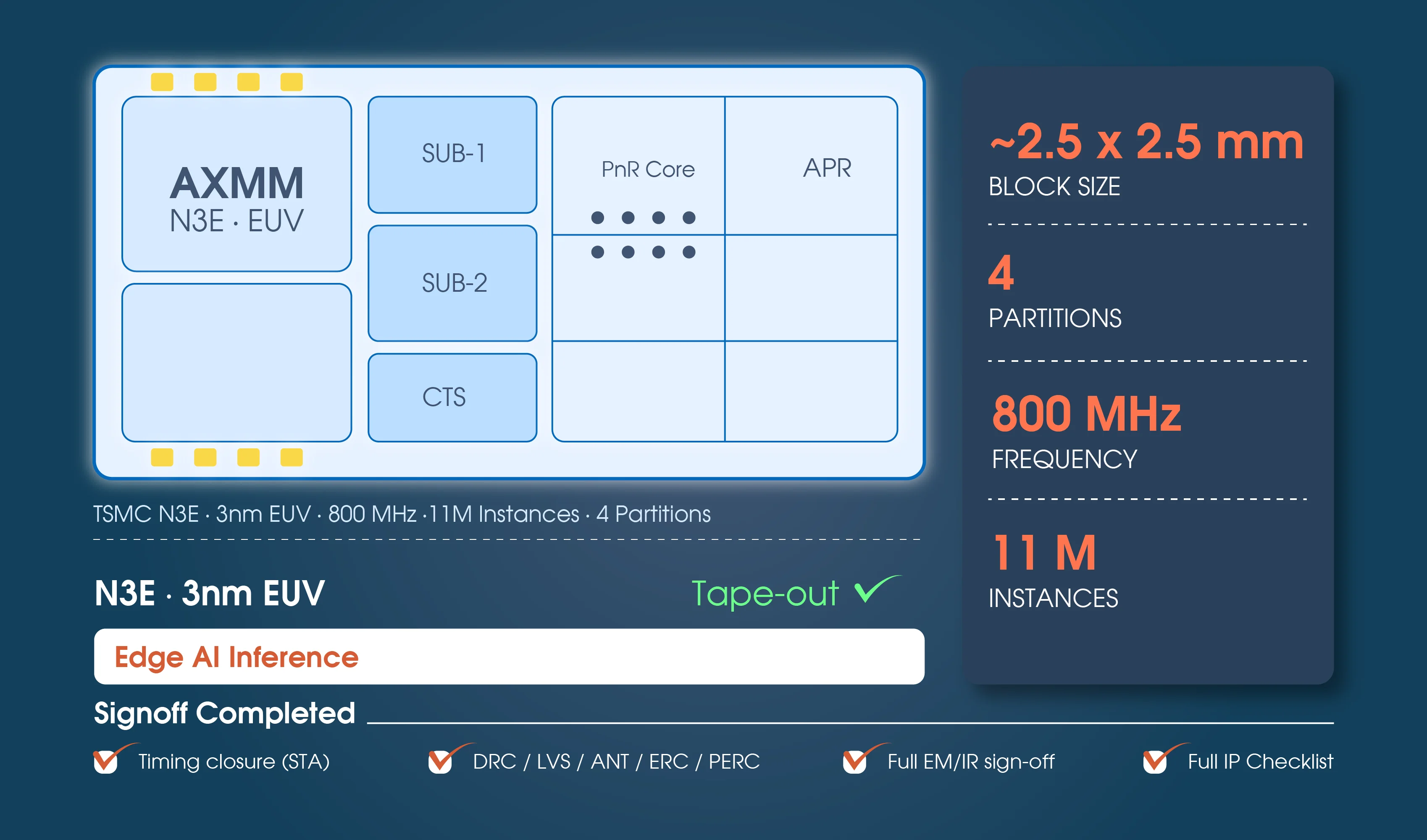
4-partition hierarchical PnR for an edge AI inference processor. IOPin budgeting, cross-partition routing congestion resolution, ELVT leakage containment, EUV multi-patterning DRC/DFM compliance, and MCMM STA sign-off on schedule.
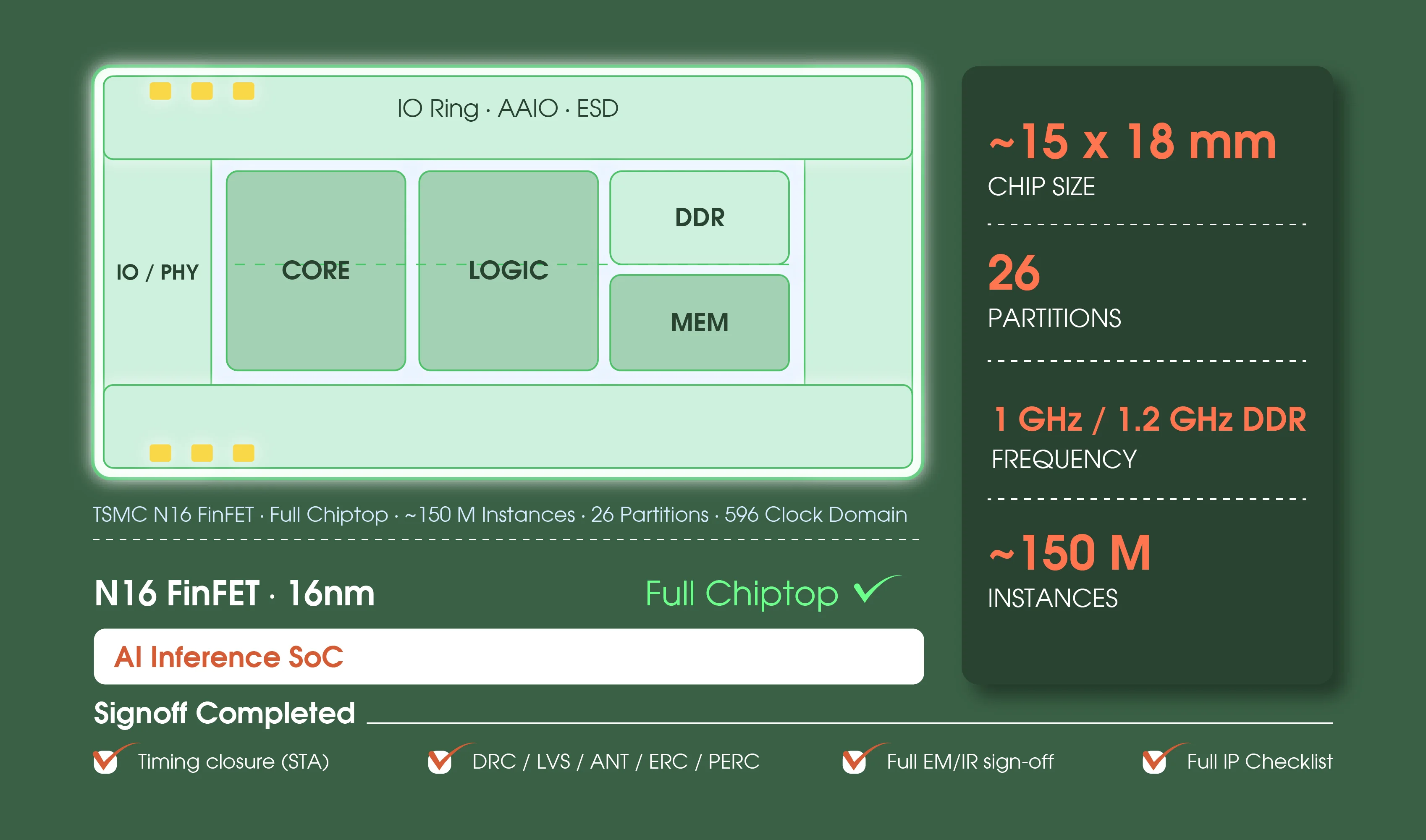
Turnkey hierarchical PnR for an AI inference SoC across 26 partitions, 8 hardened IPs, 596 clock domains. MCMM/POCV STA sign-off, EM-IR closure, custom PG mesh routing, full-chip DRC/LVS/ERC/ANT sign-off.
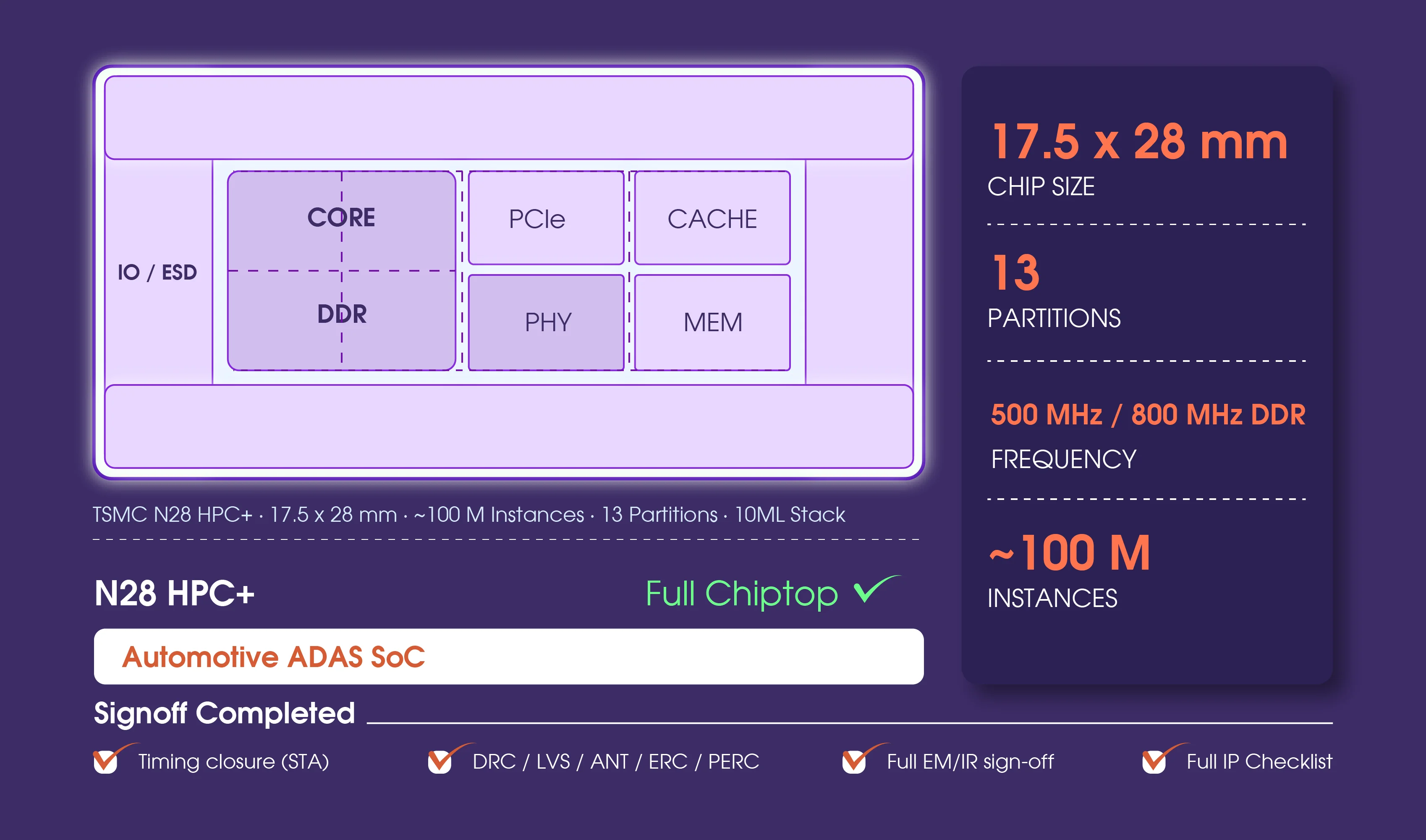
Turnkey full-chip PnR for an Automotive ADAS vision SoC. 13 partitions, 396 clock domains, 10LM5X2Y2ZUTRDL stack. AOCV MCMM STA sign-off, EM-IR closure, full DRC/LVS/ERC/ANT/ICOVL/TCD sign-off.
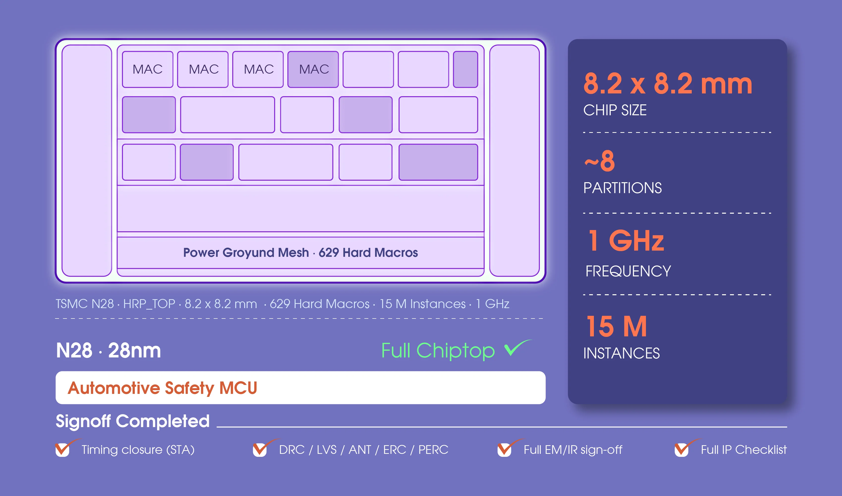
Full chiptop for an Automotive safety MCU on M1-M9 stack, 629 hard macros. AC timing and internal/interface STA sign-off at 1 GHz under narrow-channel routing congestion. Full DRC/LVS/ERC/PERC sign-off.
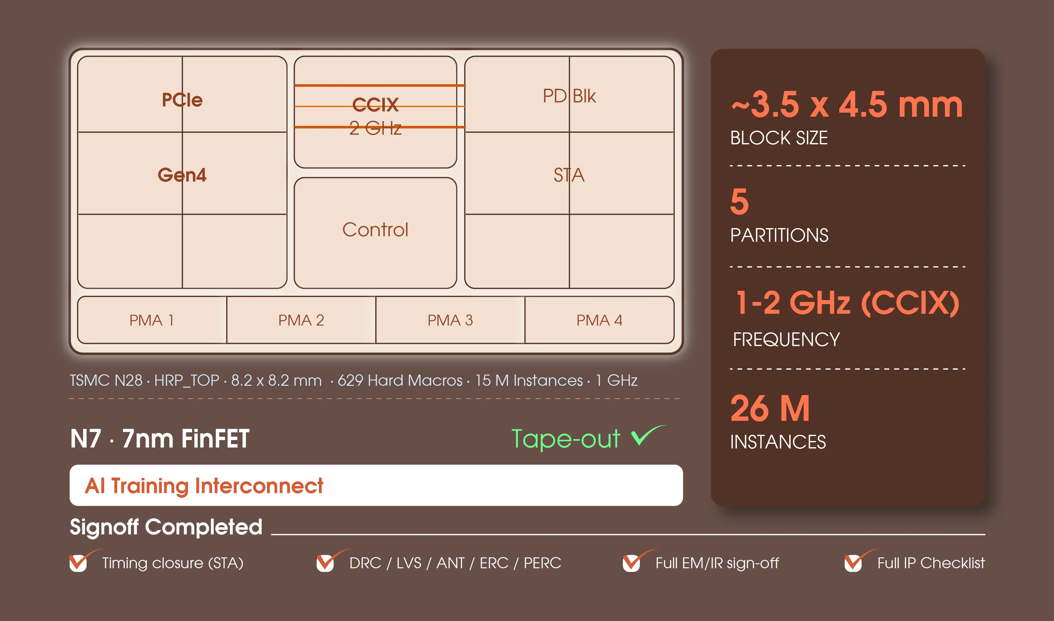
CCIX cache-coherent interconnect for AI training accelerators. Multi-source CTS across 388+412 clock domains, AOCV STA sign-off on CCIX link, 4 SerDes PMA custom routes with NDR, and full DRC/DFM sign-off.
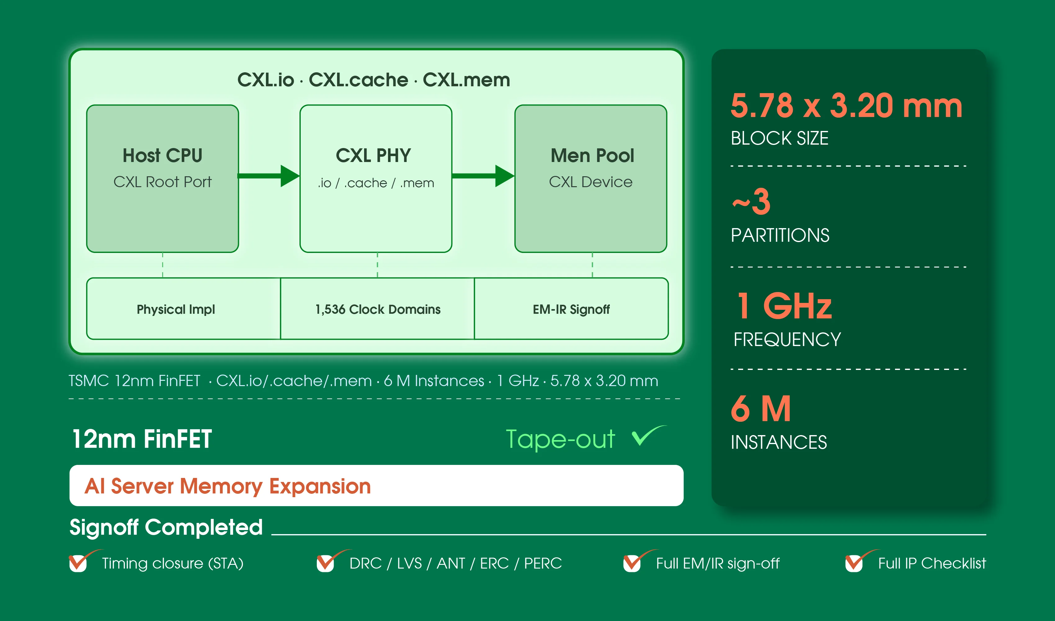
CXL protocol stack enabling AI server memory coherency and pooling. 1,536 clock domains, IP-boundary STA sign-off, EM-IR closure, post-layout parasitic extraction for STA. Full DRC/LVS sign-off.
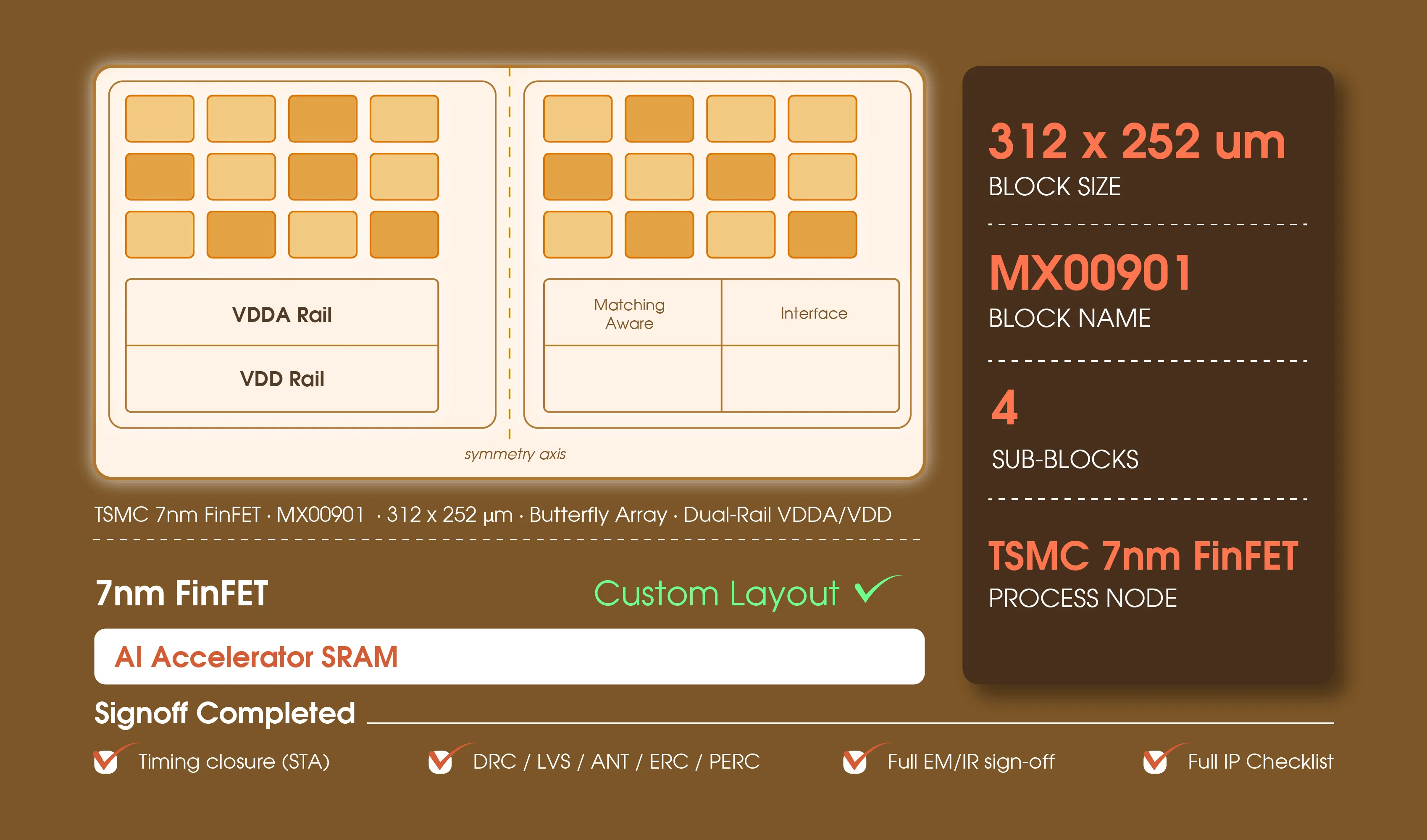
Full-custom SRAM bitcell array for AI accelerator on-chip memory. Butterfly architecture with matching-aware placement, parasitic-optimized feed-through routing, and dual-rail VDDA/VDD. DRC/LVS/ERC sign-off.
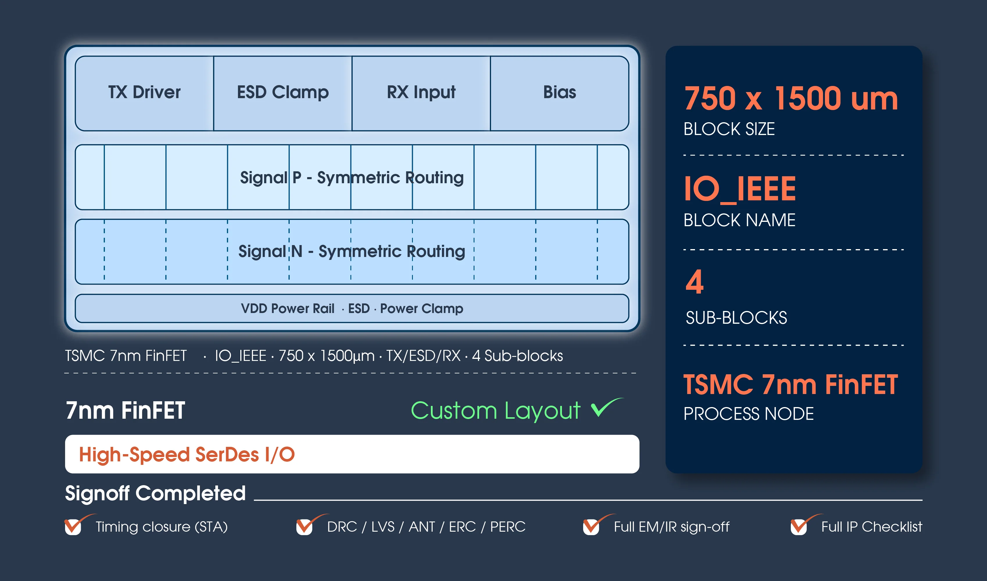
High-speed I/O pad for PCIe/SerDes interfaces. Full-custom layout with TX driver, ESD protection, RX input buffer, and power clamp. Symmetric critical-signal routing and full DRC/LVS/ICV sign-off.
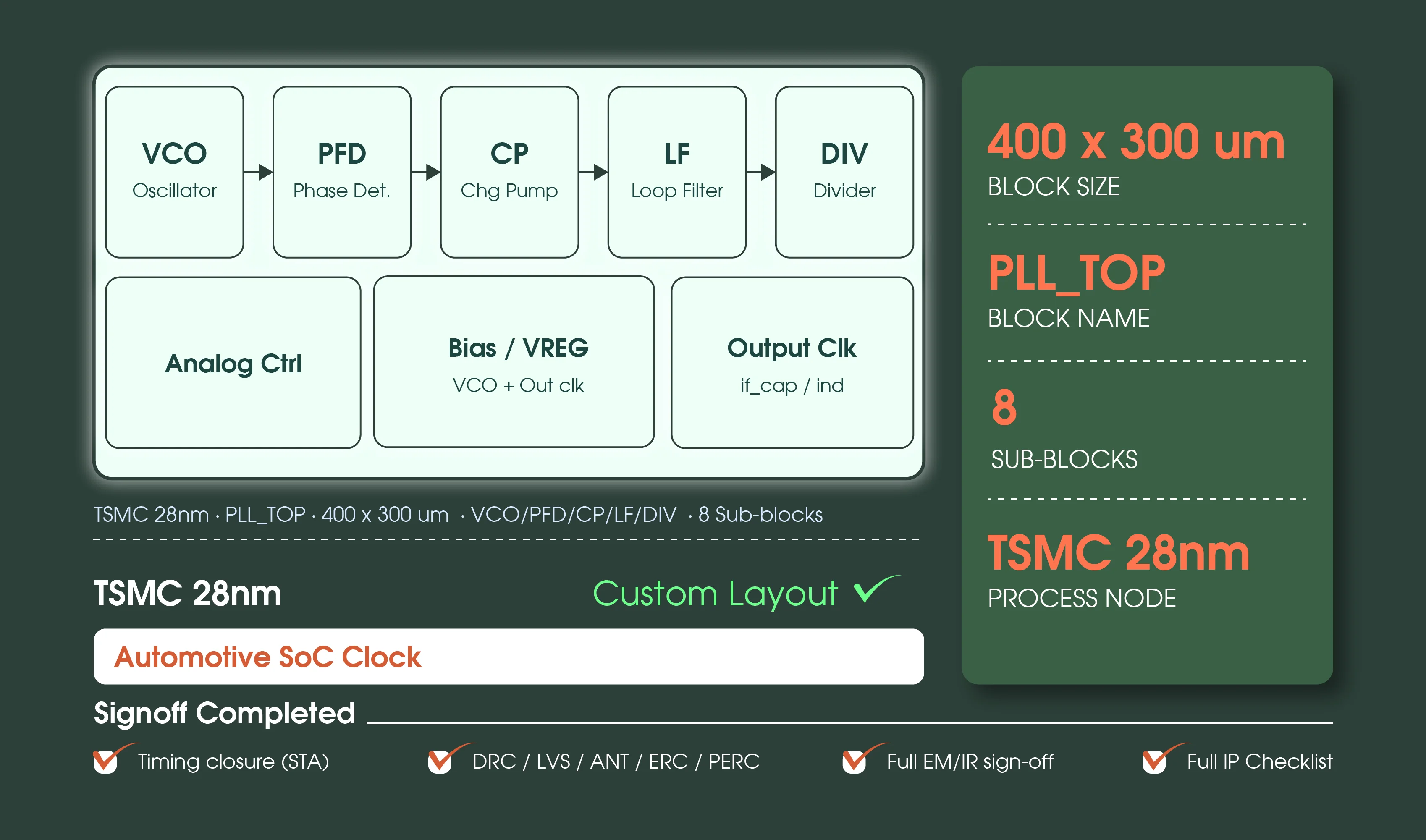
Analog PLL for Automotive and communications SoC clock generation. VCO, charge pump, loop filter capacitor/resistor, phase-frequency detector, output divider, and digital control. Matching-aware placement and VREG grid for VCO and output clocks.
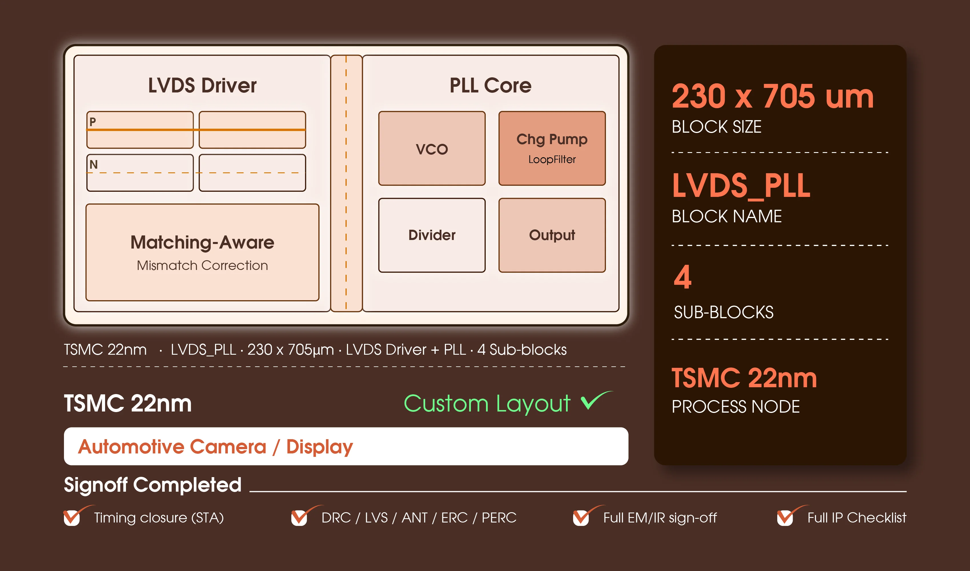
Low-voltage differential signaling with integrated PLL for Automotive camera serial link and display interface. Differential P/N matching placement, symmetric critical-path routing, and mismatch-corrected device pairs.
Ideation to production capabilities, backed by domain expertise